使用寬帶電壓和電流反饋運(yùn)算放大器時(shí)的應(yīng)用基礎(chǔ)

(Click to Enlarge Image)
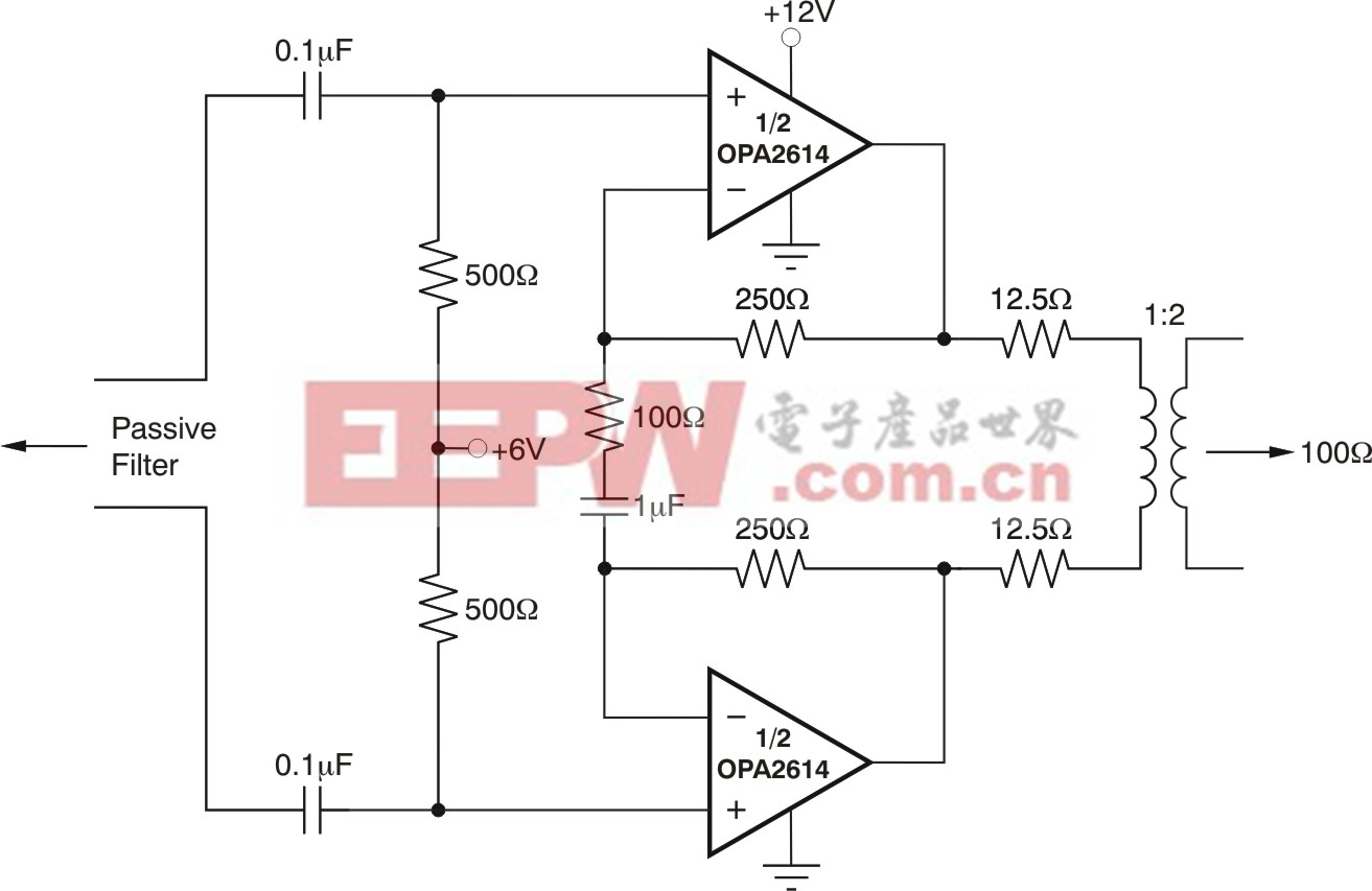
Figure 9. Wideband differencing amplifier using an OPA690.
A series resistor into the non-inverting input is then added to achieve bias current cancellation, which would only work to improve output offset voltage in a VFB implementation. This is assuming 0 Ω sources for each source and two independent sources.
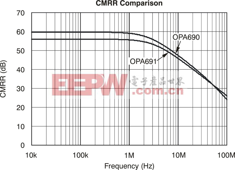
This same circuit can be built using the CFB OPA691.Figure 10shows a CMRR simulation where both inputs are tied together and driven.
(Click to Enlarge Image)
Figure 10. CMRR simulation for OPA690 and OPA691.
The resulting small output gain (large negative dB gain) is then input-referred and the negative taken to get a typical CMRR plot. The OPA690 shows slightly higher CMRR than the OPA691. In this case, the resistors of Figure 9 have been used in both simulations, and no adjustment for improved CMRR made in the OPA691 simulation.
Differential input/output circuits
An emerging class of amplifiers called fully differential amplifiers (FDA) easily can take a single or differential input signal. and produce a differential output centered on a user-selected common-mode operation point. An alternative approach in going differential-in to differential-out has been to use standard dual op amps. A brief review of that approach helps to set the background for the FDA. These approaches are useful also because once they are understood, they open up a large range of dual op amps to the designer for possible application.
Application A
Differential I/O circuits can be easily implemented using either a VFB or CFB. There is, however, some difference between a non-inverting or inverting input implementation with regard to how the common-mode voltage is treated. In the non-inverting input case, the two inputs show a high input impedance to the differential source (allowing filters or other passive circuits to be easily inserted up to these inputs). The common-mode gain from the non-inverting inputs to the differential outputs will be one.
Figure 11shows an example of this design where the wideband, high output current, dual OPA2614 is used to implement a DSL driver.
(Click to Enlarge Image)
Figure 11. Non-inverting differential I/O circuit using the OPA2614.


評論