基于MC9RS08KB12設(shè)計(jì)的8位MCU入門開發(fā)方案

MC9RS08KB12/8/4/2(RS08KB)是Freescale 公司的超低成本的入門級(jí)8位MCU,具有容易使用,設(shè)計(jì)靈活性和性能.RS08KB集成了多種外設(shè)和高效的RS08內(nèi)核,支持中斷,改善系統(tǒng)性能和節(jié)省其它元件成本. RS08KB有多達(dá)12KB閃存,256B RAM,高分辨率12路10位ADC,TPM,模塊定時(shí)器和ACMP,以提供塊速精密的檢測(cè)和控制.目標(biāo)應(yīng)用在小家電,照明控制,低檔熱控制BLDC風(fēng)扇,手持設(shè)備,電池充電器和玩具.本文介紹了MC9RS08KB12主要特性,方框圖,以及DEMO9RS08KB12演示板主要特性和電路圖.
The MC9RS08KB12/8/4/2 (RS08KB) family includes ultra-low-cost, entry-level 8-bit MCUs that balance ease of use with design flexibility and performance. The RS08KB family has an integrated peripheral set which includes a highly efficient RS08 core that supports interrupt capability, helping to improve system performance and save additional components costs. The RS08KB family eases migration by offering multiple package and flash size options, along with pin compatibility with other 5V families as well as the CodeWarrior development tool to support other 8-bit families. The family is available in 20, 16 or 8-pin packages, and features up to 12 KB flash and 254B RAM, high-resolution 12-ch., 10-bit ADC, TPM, modulo timers and ACMP to provide fast, precise sensing and control.
MC9RS08KB12主要特性:
? 8-Bit RS08 Central Processor Unit (CPU)
– Up to 20 MHz CPU at 1.8 V to 5.5 V across temperature range of –40℃ to 85℃
– Subset of HC08 instruction set with added BGND instruction
– Single Global interrupt vector
? On-Chip Memory
– Up to 12 KB flash read/program/erase over full operating voltage and temperature,12 KB/8 KB/4 KB/2 KB flash are optional
– Up to 254-byte random-access memory (RAM), 254-byte/126-byte RAM are optional
– Security circuitry to prevent unauthorized access to flash contents
? Power-Saving Modes
– Wait mode — CPU shuts down; system clocks continue to run; full voltage regulation
– Stop mode — CPU shuts down; system clocks are stopped; voltage regulator in standby
– Wakeup from power-saving modes using RTI, KBI, ADC, ACMP, SCI and LVD
? Clock Source Options
– Oscillator (XOSC) — Loop-control Pierce oscillator; crystal or ceramic resonator range of 31.25 kHz to 39.0625 kHz or 1 MHz to 16 MHz
– Internal Clock Source (ICS) — Internal clock source module containing a frequency-locked-loop (FLL) controlled by internal or external reference; precision trimming of internal reference allows 0.2% resolution and 2% deviation over temperature and voltage; supporting bus frequencies up to 10 MHz
? System Protection
– Watchdog computer operating properly (COP) reset with option to run from dedicated 1 kHz internal low power oscillator
– Low-voltage detection with reset or interrupt
– Illegal opcode detection with reset
– Illegal address detection with reset
– Flash-block protection
? Development Support
– Single-wire background debug interface
– Breakpoint capability to allow single breakpoint setting during in-circuit debugging
? Peripherals
– ADC — 12-channel, 10-bit resolution; 2.5 μs conversion time; automatic compare function; 1.7 mV/℃ temperature sensor; internal bandgap reference channel; operation in stop; hardware trigger; fully functional from 2.7 V to 5.5 V
– ACMP — Analog comparator; full rail-to-rail supply operation; option to compare to fixed internal bandgap reference voltage; can operate in stop mode
– TPM — One 2-channel timer/pulse-width modulator module; selectable input capture, output compare, or buffered edge- or center-aligned PWM on each channel
– IIC — Inter-integrated circuit bus module capable of operation up to 100 kbps with maximum bus loading; capable of higher baud rates with reduced loading
– SCI — One serial communications interface module with optional 13-bit break; LIN extensions
– MTIM — Two 8-bit modulo timers; optional clock sources
– RTI — One real-time clock with optional clock sources
– KBI — Keyboard interrupts; up to 8 ports
? Input/Output
– 18 GPIOs in 20-pin package; 14 GPIOs in 16-pin package; 6 GPIOs in 8-pin package; including one output-only pin and one input-only pin
– Hysteresis and configurable pullup device on all input pins; configurable slew rate and drive strength on all output pins
? Package Options
– MC9RS08KB12/MC9RS08KB8/MC9RS08KB4
— 20-pin SOIC, 16-pin SOIC NB or TSSOP
– MC9RS08KB2
— 8-pin SOIC or DFN
MC9RS08KB12目標(biāo)應(yīng)用:
Small appliances
Lighting control
Simple logic replacements
Low-end thermal controlled BLDC fans
Hand-held devices
Battery chargers
Toys 
圖1.MC9RS08KB12系列方框圖
DEMO9RS08KB12演示板
The 8-bit DEMO9RS08KB12 demonstration kit soldered with 20SOIC KB12, comes with everything required to complete an entire entry-level project using the RS08KB. The perfect solution that allows you to develop your next cost-effective application.
DEMO9RS08KB12演示板主要特性:
?
MC9S08KB12, 20 SOIC
?
12K Bytes Flash
?
256 Bytes RAM
?
12Ch, 10-bit ADC
?
2-Ch, Timer/PWM
?
Internal Clock Source
?
18 GPIO
?
Optional 32 kHz XTAL (not installed)
?
Integrated USB-BDM
?
BDM_PORT header for BDM cable support (not installed)
?
MCU_PORT socket header for access to MCU IO signals
?
On-board +5V regulator
?
Power Input Selection Jumpers
?
Power input from USB-BDM
?
Power input from Barrel connector and on-board regulator
?
Power Input from connector J1
?
Optional Power output through Connector J1
?
User Components Provided
Push Switches; 2 User, 1 Reset
LED Indicators; 2 User, VDD, D300
5K ohm POT w /LP Filter
Light Sensor w/ Amplifier
Jumpers
Power Select
VSEL
VX_EN
USER_EN
COM_EN
VPPE
Connectors
40-pin MCU I/O Connector
2.0mm Barrel Connector
BDM_PORT (not installed)
USB Connectors
DB9 Connector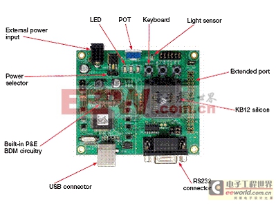
圖2.DEMO9RS08KB12演示板外形圖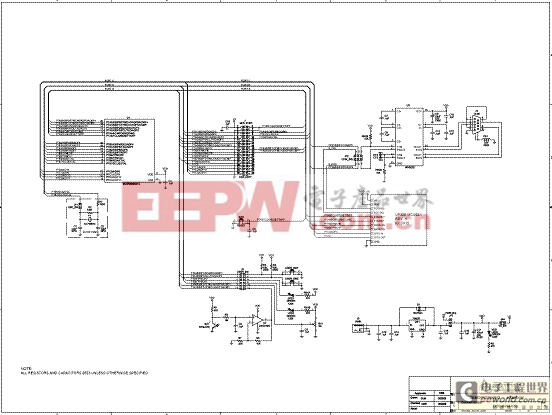
圖3.DEMO9RS08KB12演示板電路圖

評(píng)論