ADIADP2325雙路5A20V同步降壓電源解決方案

The ADP2325 is a full featured, dual output, step-down dc-to-dc regulator based on a current mode architecture. The ADP2325 integrates two high-side power MOSFETs and two low-side drivers for the external N-channel MOSFETs. The two pulse-width mod-ulation (PWM) channels can be configured to deliver dual 5 A outputs or a parallel-to-single 10 A output. The regulator operates from input voltages of 4.5 V to 20 V, and the output voltage can be as low as 0.6 V.
The switching frequency can be programmed from 250 kHz to 1.2 MHz, or it can be synchronized to an external clock to minimize interference in multirail applications. The dual PWM channels run 180° out of phase, thereby reducing input current ripple as well as reducing the size of the input capacitor.
The bidirectional synchronization pin can be programmed at a 60°, 90°, or 120° phase shift to provide for a stackable, multi-phase power solution.
The ADP2325 can be configured to operate in pulse frequency modulation (PFM) mode at a light load for higher efficiency or in forced PWM mode for noise sensitive applications. External compensation and soft start provide design flexibility.
Independent enable inputs and power-good outputs provide reliable power sequencing. To enhance system reliability, the device includes undervoltage lockout (UVLO), overvoltage protection (OVP), overcurrent protection, and thermal shutdown.
The ADP2325 operates over the ?40℃ to +125℃ junction temperature range and is available in a 32-lead LFCSP_WQ package.
ADP2325主要特性:
Input voltage: 4.5 V to 20 V
±1% output accuracy
Integrated 48 mΩ typical high-side MOSFET
Flexible output configuration
Dual output: 5 A/5 A
Parallel single output: 10 A
Programmable switching frequency: 250 kHz to 1.2 MHz
External synchronization input with programmable phase shift or internal clock output
Selectable PWM or PFM mode operation
Adjustable current limit for small inductors
External compensation and soft start
Startup into precharged output
Supported by ADIsimPowerTM design tool
ADP2325應(yīng)用:
Communications infrastructure
Networking and servers
Industrial and instrumentation
Healthcare and medical
Intermediate power rail conversion

圖1.ADP2325功能方框圖
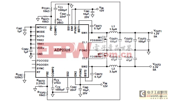
圖2.ADP2325采用外接MOSFET的應(yīng)用電路圖:VIN1 = VIN2 = 12 V, VOUT1 = 1.2 V, IOUT1 = 5 A, VOUT2 = 3.3 V, IOUT2 = 5 A, fSW = 500 kHz
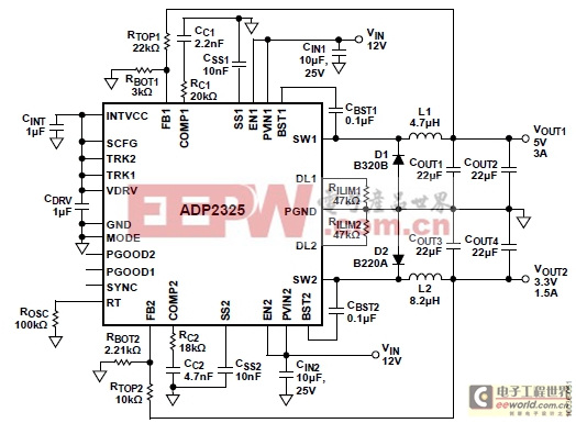
圖3.ADP2325采用外接二極管的應(yīng)用電路圖:VIN1 = VIN2 = 12 V, VOUT1 = 5 V, IOUT1 = 3 A, VOUT2 = 3.3 V, IOUT2 = 1.5 A, fSW = 600 kHz
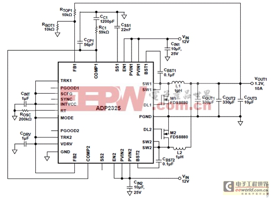
圖4.ADP2325并聯(lián)單輸出應(yīng)用電路圖: VIN = 12 V, VOUT = 1.2 V, IOUT = 10 A, fSW = 300 kHz
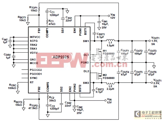
圖5.ADP2325采用MODE引腳下拉到GND的使能PFM模式應(yīng)用電路圖:VIN1 = VIN2 = 12 V, VOUT1 = 1.5 V, IOUT1 = 5 A, VOUT2 = 2.5 V, IOUT2 = 5 A, fSW = 600
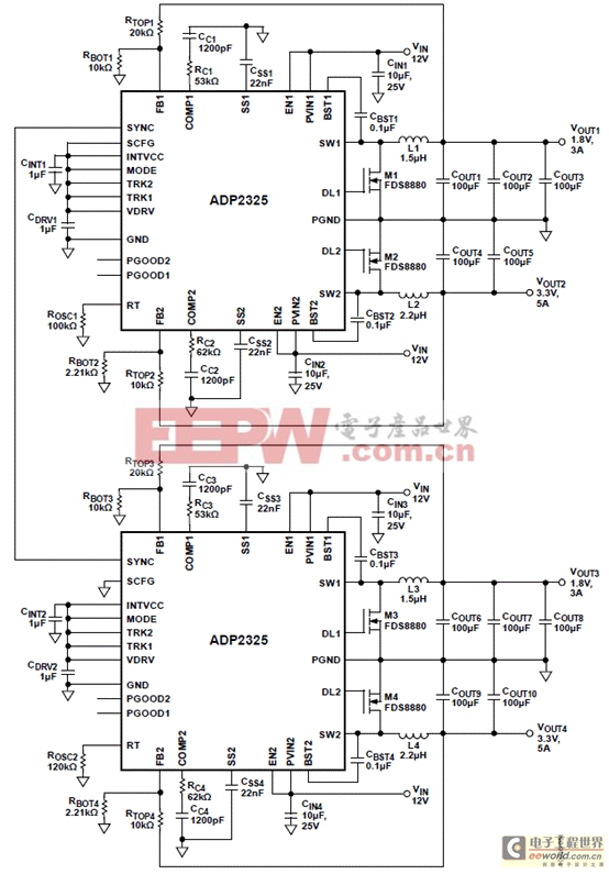
圖6.ADP2325每路間90度相移的同步應(yīng)用電路圖
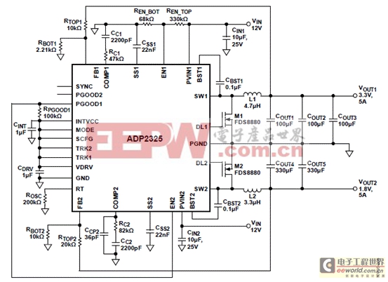
圖7.ADP2325可編VIN_RISING = 8.7 V, VIN_FALLING = 6.7 V應(yīng)用電路: 3.3 V 先于1.8V起動, VIN1 = VIN2 = 12 V, VOUT1 = 3.3 V, IOUT1 = 5 A, VOUT2 = 1.8 V, IOUT2 = 5 A, fSW = 300 kHz
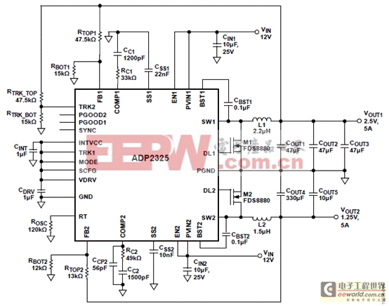
圖8.ADP2325通路2跟蹤通路1應(yīng)用電路圖: VIN1 = VIN2 = 12 V, VOUT1 = 2.5 V, IOUT1 = 5 A, VOUT2 = 1.25 V, IOUT2 = 5 A, fSW = 500 kHz
ADP2325評估板ADP2325-EVALZ
Evaluation Board for the ADP2325, Dual 5 A, 20 V, Synchronous Step-Down Regulator with Integrated High-Side MOSFET
The ADP2325 evaluation board, ADP2325-EVALZ, is a complete, dual, 5 A step-down regulator solution that allows users to evaluate the performance of the ADP2325 with a near ideal printed circuit board (PCB) layout.
The two pulse-width modulation (PWM) channels can be configured to deliver dual, 5 A outputs or a parallel-to-single, 10 A output. The switching frequency can be programmed between 250 kHz and 1.2 MHz, or it can be synchronized to an external clock with a programmed 60°, 90°, or 120° phase shift, which provides the possibility for a stackable multiphase power solution.
The outputs of the ADP2325 evaluation board are preset to 1.2 V and 3.3 V for Channel 1 and Channel 2, respectively. With the PWM mode selected, the switching frequency is set to 500 kHz. Different output voltage settings and configurations can be achieved by changing appropriate passive components or jumper settings. The ambient temperature operating range is ?0℃ to +85℃.
評估板ADP2325-EVALZ主要特性:
Input voltage: 4.5 V to 20 V
±1% output voltage accuracy
Integrated 48 mΩ typical on-resistance high-side MOSFET
Flexible output configuration
Dual output: 5 A/5 A
Parallel single output: 10 A
Programmable switching frequency: 250 kHz to 1.2 MHz
External synchronization input with programmable phase shift, or internal clock output
Selectable PWM or PFM mode operation
Adjustable current limit for small inductor
External compensation and soft start
Startup into precharged output
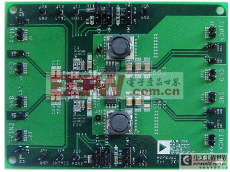
圖9.評估板ADP2325-EVALZ外形圖
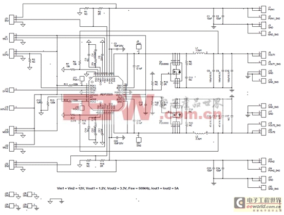
圖10.評估板ADP2325-EVALZ電路圖
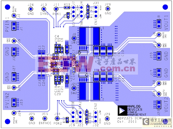
圖11.評估板ADP2325-EVALZ PCB元件布局圖:頂層
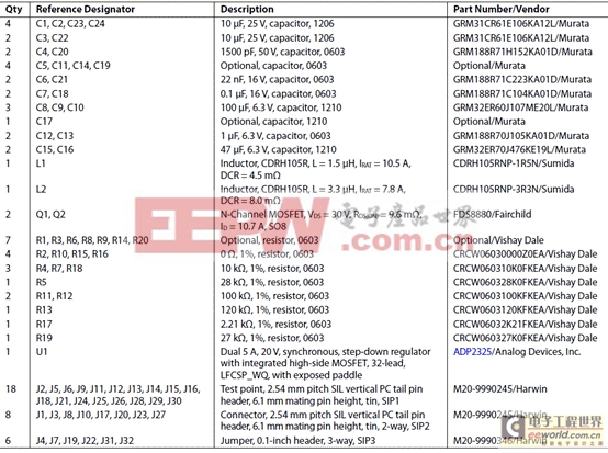
評估板ADP2325-EVALZ材料清單(BOM):
詳情請見:
http://www.analog.com/static/imported-files/data_sheets/ADP2325.pdf
和
http://www.analog.com/static/imported-files/user_guides/UG-374.pdf


評論