Power Integrations TOPSwitch-HX電源解決方案

Power Integrations公司的TOPSwitch-HX系列是成本效益器件,在單個器件內(nèi)集成了700V功率MOSFET,高壓開關(guān)電流源,PWM控制,振蕩器,熱關(guān)斷電路,故障保護以及其它控制電路.通用交流電壓輸入,在不加散熱器的情況下,輸出功率可高達35W,待機輸入功率1W時的輸出功率,在110V AC時大于600mW,而在265V AC輸入時大于500mW.本文介紹了該系列中的TOP254-258系列的主要性能特點,以及進行開關(guān)電源設(shè)計所需的材料,包括各種應用電路圖。
本文引用地址:http://www.butianyuan.cn/article/78260.htmTOP254-258 TOPSwitch-HX Family
TOPSwitch-HX cost effectively incorporates a 700 V power MOSFET, high voltage switched current source, PWM control, oscillator, thermal shutdown circuit, fault protection and other control circuitry onto a monolithic device.
產(chǎn)品亮點:
Lower System Cost, Higher Design Flexibility
Multi-mode operation maximizes effi ciency at all loads
No heatsink required up to 35 W using P, G and M packageswith universal input voltage and up to 48 W at 230 VAC
Output overvoltage protection (OVP) is user programmable for latching/non-latching shutdown with fast AC reset
Allows both primary and secondary sensing
Line undervoltage (UV) detection prevents turn-off glitches
Line overvoltage (OV) shutdown extends line surge limit
Accurate programmable current limit
Optimized line feed-forward for line ripple rejection
132 kHz frequency (Y package) reduces transformer and power supply size
Half frequency option in Y package for video applications
Tight I2f parameter tolerance reduces system cost
Maximizes MOSFET and transformer power delivery
Minimizes overload power, reducing cost of transformer,primary clamp and secondary components
Frequency jittering reduces EMI fi lter cost
Improved auto-restart delivers <3% of maximum power in short circuit and open loop fault conditions
Accurate hysteretic thermal shutdown function automatically recovers without requiring a reset
Fully integrated soft-start for minimum start-up stress
Pin-out simplifi es heatsinking to the PCB for P, G and M packages
Extended creepage between DRAIN and all other pins improves field reliability
Heatsink is connected to SOURCE for low EMI
Energy efficient over entire load range
No-load consumption <200 mW at 265 VAC
Standby power for 1 W input
>600 mW output at 110 VAC input
>500 mW output at 265 VAC input
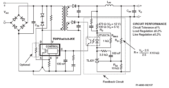
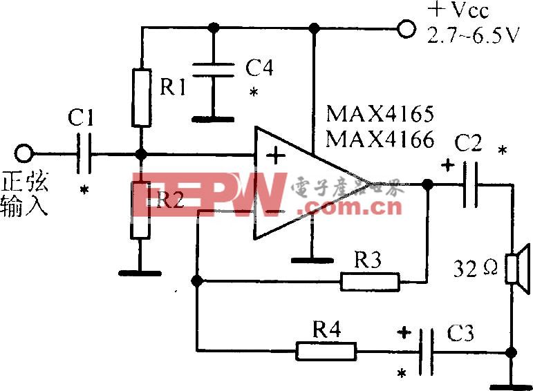
圖1.采用Opto/TL/431反饋的TOPSwitch-HX反激電源方框圖.
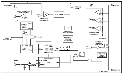
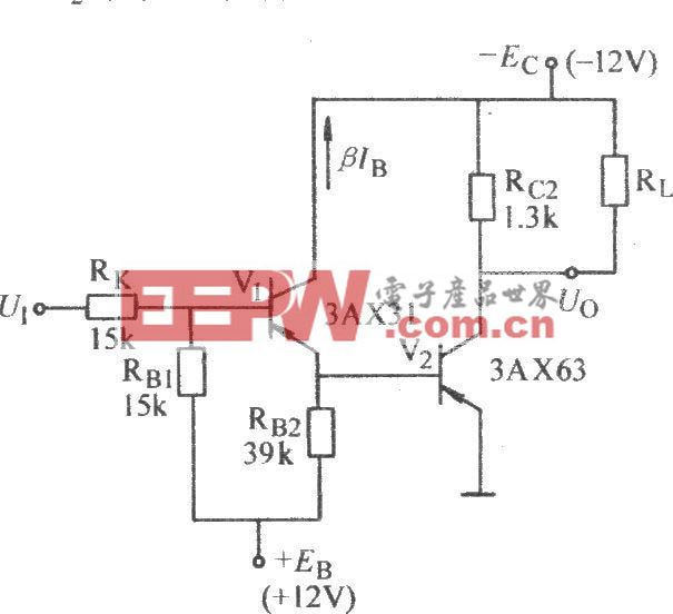
圖2a.P和G封裝的TOP254-258功能方框圖.
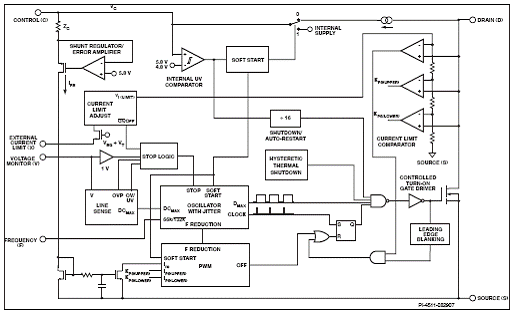
圖2C.Y封裝的TOP254-258功能方框圖.
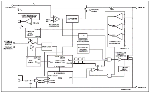
圖2b.M封裝的TOP254-258功能方框圖.
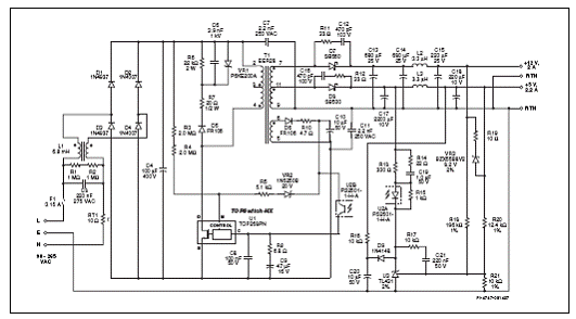
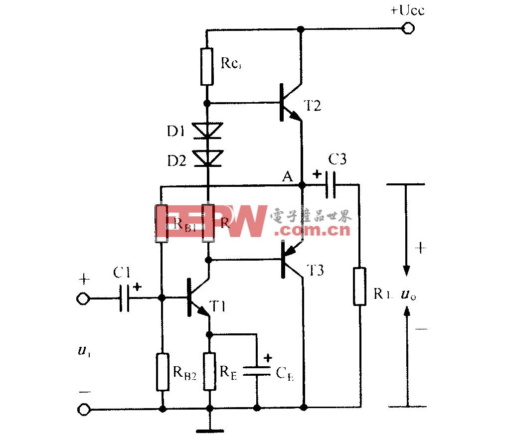
圖3.采用TOP258PN的35W雙輸出電路圖.

圖4.采用TOP258YN的150W,19.5V電源電路圖.

圖5.采用TOP258MN的20W(連續(xù)),80W(峰值)通用輸入電源電路圖.
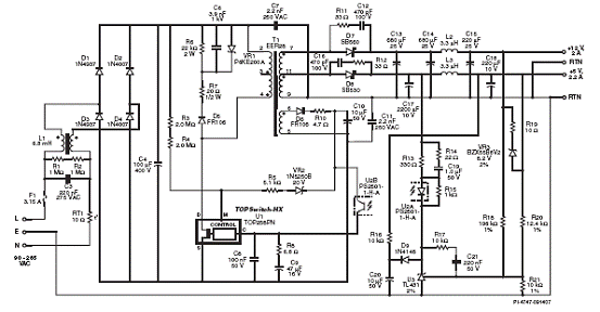
圖6.采用TOP258PN的通用輸入35W電源電路圖.


評論