新增高電壓能力的MAX471/MAX472高側(cè)電流檢測放大器

The MAX471 and MAX472 are complete bi-directional high-side current sense amplifiers for portable PCs, telephones, and other systems where battery/DC line monitoring is important, and where ground continuity between system and supply is crucial.
However, the part's 36V maximum operating voltage is a limiting factor when higher voltage systems are to be monitored, such as traction motor batteries and telecom central exchange power supplies, both of which require operation above 72V. New high-side current sense amplifiers such as the MAX4080, can operate up to 76V.
The circuit of Figure 1 shows a simple way to add high voltage capability to the basic MAX471/2. Low supply current of the current monitor (100μA) allows a very simple floating power supply formed by avalanche diode D1, C1, C2, and the NPN current source Q1 and Q2. The voltage compliance of the current source provides the high voltage capability. With the part shown, Motorola MPSA42 (Q1), 300V is the maximum recommended, giving an absolute maximum input voltage rating for the whole circuit of 305.1V. Use of a 33V avalanche diode for D1 pushes this to 333V.
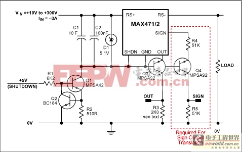
Figure 1. High voltage MAX471/2.
The OUT pin of the MAX471/2 is a current source of 500μA/A, whose output impedance is typically 3MΩ. A PNP common base stage, Q3, provides the high voltage compliance while retaining the ground reference capability of the output. An MPSA92 is complimentary to the MPSA42 and provides a matching 300V operation. Collector resistor R3 may be chosen to provide a particular full scale output voltage. With the prototype values chosen, the output voltage at Q3 collector changed by 10mV for an input voltage range of +10V to +300V.
A simple two transistor current source, Q1 and Q2, is accurate enough and is sufficient to provide voltage compliance and diode current. Chose the current value to ensure that the avalanche diode is regulating. 1mA was chosen for the prototype. The voltage supply to R1 biases the current source, and provides a suitable ground referenced point with which to switch off the whole circuit.
The common base stage Q3 allows the same scaling factors, as calculated for the MAX471/2, to be used at the collector with little additional error loss. Remember that the current gain for a common base stage is α, and is 1. Its value may be obtained from the DC β-spec in the transistor data sheet, namely
For the MPSA92, β(min) = 25, giving a figure for α(min) = 0.96. This can be improved by increasing the current gain of Q3, either with a Darlington or compound transistor connection.= β / (1 + β)
The MAX471/2 have a polarity output, which signals the direction of the current through the sense terminals. Adding Q4, another common base PNP stage adds high voltage compliance, and produces a ground referenced logic level output.


評論