How to Use High-Voltage and High-Current-Drive Op Amps in 4–20mA Current-Loop Systems
Abstract: This article shows how to use a high-voltage, high-current-drive operational amplifier to convert a voltage signal into a ±20mA or 4–20mA current signal for use in process-control industrial applications. The MAX9943 op amp serves as the example device. Experiments are described and test results presented.
Introduction
Current loops have long been used in process-control industrial applications. Current loops enable the transfer of information from remote sensors to central processing units, or from those central units to remote actuators. Although 4–20mA current loops are quite common for the application, ±20mA current loops can be used as well. For low-impedance loads, the use of a high-voltage op amp with a high-current-drive output simplifies the circuit design by eliminating the need for external power FETs.
This article shows how to use a high-voltage, high-current-drive op amp in a 4–20mA current-loop application. The op amp converts a voltage signal from a DAC into a ±20mA or 4–20mA current output. Application experiments feature the MAX9943 op amp. Test data are presented.
Basics of a current loop
A current loop typically includes a sensor, transmitter, receiver, and an ADC or microcontroller (Figure 1). The sensor measures a physical parameter (such as pressure or temperature) and provides a corresponding output voltage. The transmitter converts the sensor's output into a proportional 4mA-to-20mA current signal. The receiver then converts the 4–20mA current into a voltage. An ADC or a microcontroller digitizes the receiver's voltage output.
Figure 1. These major components form a simple current loop.
In current loops the information is transmitted by a current-modulated signal. For 4–20mA systems, 4mA normally represents the sensor's zero-value output while 20mA represents the full-scale output. A broken loop (0mA, a fault condition) can be easily distinguished from the sensor's zero output (4mA).
Current loops are inherently more immune to noise than voltage-modulated signals. This is why they are ideal for use in noisy industrial environments. The signal can travel over long distances and information can be sent to, or received from, remote locations. Typically the sensor is remote from the control center where the system microcontroller is located.
A more complex system includes a second current loop from the microcontroller or DSP to an actuator (Figure 2). A DAC converts the digital information into an analog voltage signal. A current-loop transmitter converts the DAC's output voltage into a 4–20mA or ±20mA current signal that drives the actuator. An example of such a system can be found in power-grid monitoring systems where sophisticated algorithms determine the current state of the system, predict the direction of changes in the system, and implement a control loop to dynamically adjust the system.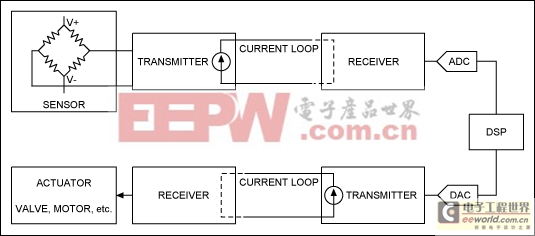
Figure 2. A more complex system uses a second current loop for controlling an actuator.
Use the op amp as a VI converter with a high-current drive
The circuit of Figure 3 shows how a simple VI (voltage-to-current) converter can be designed with two op amps and a few external resistors. When powered with ±15V, the op amp (here, the MAX9943) delivers more than ±20mA output current to small impedance loads.
The MAX9943 is a 36V op amp with a high-output current drive. It is stable with up to 1nF load capacitance. The device is ideal for industrial applications where a voltage signal coming from a DAC needs to be converted into a proportional 4–20mA or ±20mA current signal.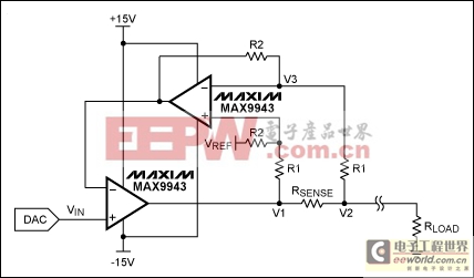
Figure 3. A VI converter transforms the DAC output to load current. The circuit uses two MAX9943 op amps.
The relationship between the input voltage, VIN, and the load current is given by Equation 1:
| VIN = (R2/R1) × RSENSE × RLOAD + VREF | (Eq. 1) |
In this circuit example the component values are:
R1 = 1kΩ
R2 = 10kΩ
RSENSE = 12.5Ω
RLOAD = 600Ω
A typical load value would be in the order of several hundred ohms. However, significantly smaller impedance loads can occur either from short-to-ground faults, or to allow long-distance signal transmission by reducing the voltage burden requirements at the receiver.
VREF can be synchronized with the reference voltage used by the DAC. In that case all voltages (VIN) are ratiometric with VREF, and errors from variation in VREF can be eliminated.
Create a ±20mA current drive from a ±2.5V range
The circuit in Figure 3 can also be used to create a ±20mA current drive. With VREF = 0V, the input range between -2.5V and +2.5V produces a nominal ±20mA current output, as shown in Figure 4.
The relationship between the input voltage (VIN) and the output voltage (V1) of the "forward" op amp is given by:
| VIN = (R2/R1) × (1 - α/β) × V1 + VREF × (1 – (R2/R1) × 1/(β × (R2 + R1))) | (Eq. 2) |
Where:
| α = (1/RSENSE) + R2/(R1 × (R1 + R2)) | (Eq. 3) |
| β = 1/RSENSE + (1/R1) + 1/RLOAD | (Eq. 4) |
Using the component values specified in Equations 2 and 3:
| V1 = 4.876 × VIN - 4.872 × VREF | (Eq. 5) |
The relationship in Equation 5 helps to avoid saturating the output devices. In fact, when VIN = +2.5V, the output of the lower op amp (V1) reaches about 12.2V. If the input voltage increases beyond 2.5V, eventually the output device reaches its saturation point and the output voltage can no longer increase. The Figure 4 curves flatten and no longer follow the ideal profile. A similar process happens when the negative input is lowered below -2.5V.
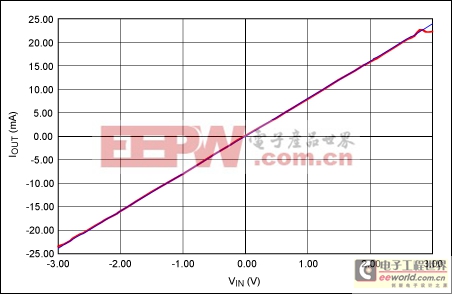
Figure 4. A ±20mA output current range is produced by a ±2.5V input voltage range. The blue line is the ideal gain curve; the red line is the measured data. VCC = +15V; VEE = -15V.
The Figure 4 data show that the MAX9943 still operates in the linear range when sourcing and sinking up to about ±21.5mA, which corresponds to the input of ±2.68V and of ±13V at the output of the forward (lower) op amp. The negative current could actually be a much larger magnitude because the MAX9943's output voltage can operate very close to the negative supply voltage. The device is limited to about 2V from the positive supply. (The 2V value depends on the load, and is given as a worst-case specification vs. process and temperature.)
Some applications require higher output current, either to satisfy margin concerns or to provide room for calibration. For those applications the Figure 3 circuit can be operated with dual ±18V supply voltages (instead of ±15V). Now the op amp can drive up to ±24mA (corresponding to ±3V inputs) and remain in the linear zone. This performance is illustrated in Figure 5.
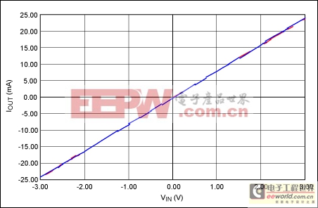
Figure 5. A ±24mA output current range is produced by a ±3V input voltage range. The blue line is the ideal gain curve; the red line is the measured data. VCC = +18V; VEE = -18V.
Create a 4–20mA current drive from a 0 to 2.5V range
Referring back to Equation 5, when VREF = -0.25V the input range between 0V and +2.5V produces a 2mA-to-22mA current output (Figure 6). Normally in 4–20mA current loops, designers want extra "room" in the dynamic range (e.g., from 2mA to 22mA) to allow for software calibration. If more current is required, then the MAX9943 circuit can be powered with a dual ±18V supply voltage, as explained earlier.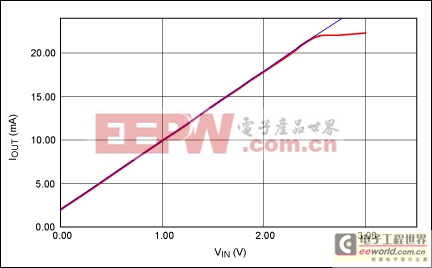
Figure 6. A 4–20mA output current range is produced by a 0V to 2.5V input voltage range. The blue line is the ideal gain curve; the red line is the measured data. VCC = +15V; VEE = -15V.
Conclusion
Current loops are very popular for industrial applications that need to transfer information from remote sensors to central processing units, or from those central units to remote actuators.
The MAX9943 op amp has been shown to be ideal for control-loop applications where a voltage from a sensor or a DAC needs to be converted into either a 4–20mA or ±20mA current range. The MAX9943 offers a precision, high-current drive over the temperature range. It is stable with capacitive loads up to 1nF, as are found in long transmission lines.





評(píng)論