設(shè)計(jì)基于LED的視頻顯示板,Designing an LED
Before the Windows operating system recognizes a monitor, it probes the monitor through DDC using an I2C protocol. The monitor then responds with its EDID that contains manufacturing and operations information. Similarly, the AT24C02 EEPROM is used to store the EDID information for the LED video-display board. The manufacturer's ID must be obtained from the Video Electronics Standards Association (VESA). For this reference design, the EDID of a DVI-capable LCD monitor is borrowed and stored into the AT24C02 EEPROM. When all of its three address pins are grounded, the I2C device address of the AT24C02 EEPROM is 0xA0, which is what the operating system will be searching for.
More detailed image (PDF, 160kB)
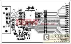
Figure 5. DVI receiver PCB (2.25" x 4").
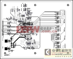
The FPGA board (Figure 6) consists mainly of two SRAMs, and a single Altera? FPGA device. Both LVDS interface and memory access functions reside inside the FPGA. The FPGA's main purpose in this design is the demultiplexing of DVI digital video information. Another important function of the FPGA is data-frame recognition for configuration, global intensity PDM, and CALDAC information. These data frames, containing other than the individual PWM information, are received and directly sent to the corresponding MAX6974 registers once a video control frame is identified.
More detailed image (PDF, 304kB)
Figure 6. FPGA PCB (7.5" x 9.5").
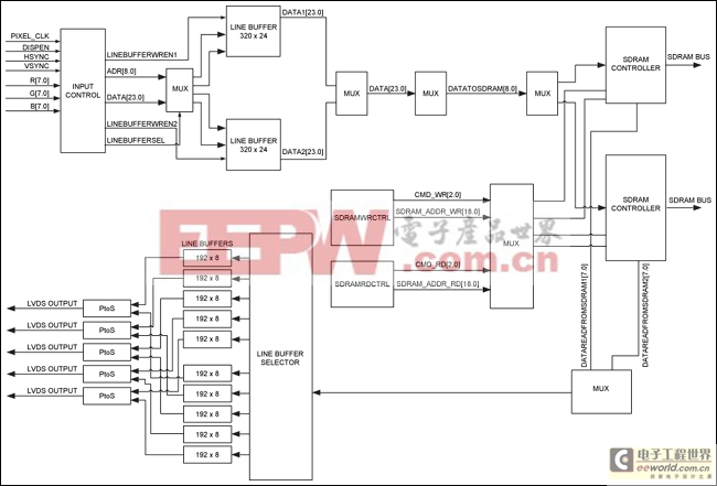
Figure 7shows the internal functional blocks of the FPGA. A screen frame of the pixel bits is stored in the SRAMs for buffering. Line buffers implemented inside the FPGA are used to interface the TFP401A DVI receiver and the LVDS channels. Two line buffers, one for accepting data bits from the TFP401A DVI receiver and the other for transferring to the SRAM, are used to accept data from the TFP401A DVI receiver. Similarly, two line buffers are used for each LVDS channel. The FPGA provides combination logic circuits to meet the timing requirements for matching both DVI and LVDS data throughputs and for all necessary SRAM data, address, and control signals. Because the SRAM is a single-port type, while both Read and Write operations are carried out simultaneously, a memory-access-scheduling mechanism is also implemented inside the FPGA.
More detailed image (PDF, 56kB)
Figure 7. FPGA internal functional blocks.
Each MAX6974 drives eight RGB LEDs. Each display module board (Figure 8) contains 64 MAX6974 LED drivers in eight rows and eight columns, plus 512 RGB LEDs in eight rows and 64 columns. All LEDs are assembled on one side of the PCB with an LED center-to-center distance of 8mm from their top, bottom, left, and right neighbors. The dimensions of the display module board are 512mm x 64mm. All MAX6974 devices are assembled on the other side of the PCB. On the same side where MAX6974 devices are assembled, power and ground pins, as well as 1 x 6 headers, are also installed. Two 1 x 6 headers are installed: one for the LVDS input interface at the top left corner, and the other for the LVDS output interface at the bottom left corner. The display module board is designed to be snapped on to a display board frame where interconnection boards are installed. No additional wiring is required for the LVDS interface between adjacent LED display module PCBs.

More detailed image (PDF, 1.25MB)
Figure 8. LED display module PCB (64mm x 512mm) with the LEDs assembled on one side and the MAX6974 LED drivers on the other side. (The PCB is broken into left (a) and right (b) sides.)
Figure 9shows the general assembly of the QVGA LED video-display board with a DVI receiver, an FPGA, and 150 LED display module PCBs. These PCBs are arranged in 5 columns and 30 rows. DVI receiver and FPGA PCBs are shown on the top of the video-display board assembly. They can easily be hidden behind the LED display module PCBs in the top rows.
More detailed image (PDF, 60kB)
Figure 9. Video-display board assembly.
Power Consumption
The operating current for each MAX6974 device is 28mA (CALDAC inactive) or 54mA (CALDAC active) from a 3.3V VCCsupply. The operating current for 64 MAX6974 LED drivers on an LED display module PCB is 1.8A or 3.5A. The maximum LED current through each MAX6974 port is 30mA from a 5V VLEDsupply. The maximum LED current for each LED display module PCB with 512 RGB LEDs is 46A. Multiple 3.3V and 5V supplies are necessary to provide power for the entire video-display board.An 80 x 64 LED Video Brick
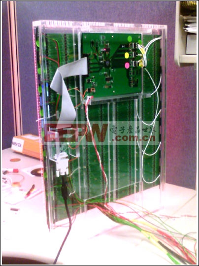
Figure 10shows 9 LED PCBs assembled in an acrylic frame (capable of fitting 10 PCBs) with FPGA and DVI receiver PCBs mounted in the back (seeFigure 11). The entire QVGA display board can be assembled using 15 (3 x 5) such acrylic frames.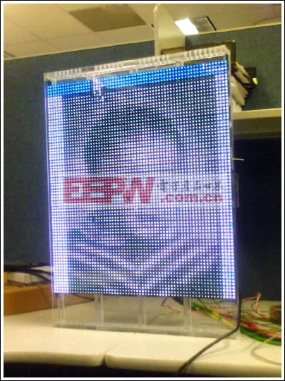
Figure 10. An acrylic frame that houses up to 10 LED PCBs.





評(píng)論