ST STHV748高性能超聲波脈沖控制方案
ST 公司的STHV748是4路5級(jí)±90V, 2 A高性能高速超聲波脈沖控制器,輸出電壓從0V到90V,工作頻率高達(dá)20MHz,抖動(dòng)低至20ps,具有抗交叉導(dǎo)通功能和低2次諧波失真特性,STHV748應(yīng)用在醫(yī)療超聲波圖像,脈沖發(fā)生器,NDT超聲波發(fā)送和壓電傳感器驅(qū)動(dòng)器.本文介紹STHV748主要特性,方框圖和典型應(yīng)用電路.
本文引用地址:http://butianyuan.cn/article/198854.htmWorld’s Most Integrated High-Performance Ultrasound Pulse Controller
STHV748: 5-level, ±90 V, 2 A high-speed pulser with four independent channels
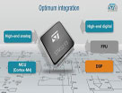
This monolithic, high-voltage, high-speed pulser generator features four independent channels. It is designed for medical ultrasound applications, but can also be used for other piezoelectric, capacitive or MEMS transducers. The device comprises a controller logic interface circuit, level translators, MOSFET gate drivers, noise blocking diodes and high-power P-channel and N-channel MOSFETs as output stage for each channel,clamping-to-ground circuitry, anti-leakage, antimemory effect block, thermal sensor and HV receiver switch (HVR_SW) which guarantees a strong decoupling during transmission phase.Moreover the STHV748 includes self biasing and thermal shutdown blocks .
Each channel can support up to five active output levels with two half bridges. The output stage of each channel is able to provide ±2 A peak output current. In order to reduce power dissipation during continuous wave mode, the peak current is limited to 0.6 A.
STHV748主要特性:
■ High-density ultrasound transmitter
■ 0 to ±90 V output voltage
■ Up to 20 MHz operating frequency
■ Low-power, high-voltage drivers
■ 2 independently supplied half bridges for each channel in pulse wave (PW) mode
– 5-level output waveform
– ±2 A source and sink current
– Down to 20 ps jitter
– Anti-cross conduction function
– Low 2nd harmonic distortion
– Fine-tuning on propagation delay
■ Fully integrated clamping-to-ground function
– 6 Ω synchronous active clamp
– Anti-leakage on output node
■ Dedicated half bridge for continuous wave (CW) mode on each
– Down to 0.1 W power consumption
– ±0.6 A source and sink current
– Down to 10 ps jitter
■ Fully integrated HV receiver switch
– 13.5 Ω on resistance
– HV MOS topology to minimize current consumption
– Up to 300 MHz BW
■ 2.4 V to 3.6 V CMOS logic interface
■ Auxiliary integrated circuits
– Noise blocking diodes
– Fully self-biaising architecture
– Anti-memory effect for all internal HV nodes
– Thermal protection
– Stand by function
■ Latch-up free due to HV SOI technology
■ Very few external passive components needed
STHV748應(yīng)用:
■ Medical ultrasound imaging
■ Pulse waveform generator
■ NDT ultrasound transmission
■ Piezoelectric transducers driver
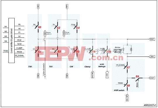
圖1.STHV748單路方框圖
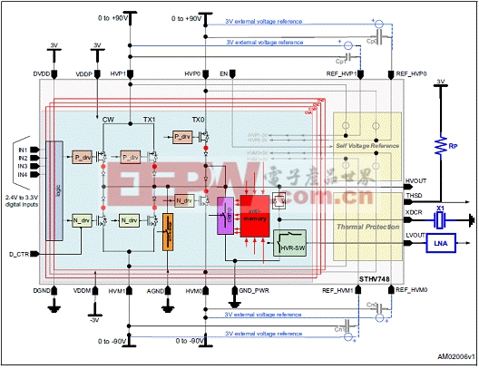
圖2.STHV748典型應(yīng)用電路
詳情請見:
http://www.st.com/stonline/products/literature/ds/15450.pdf




評(píng)論